
Device Recovery and Reverse Engineering
Recovering and re-manufacturing undocumented devices — schematic reconstruction, replacing obsolete components with modern equivalents, a new board revision.
Typical project:Recovery of an undocumented industrial board· 2–5 weeks
Project
Tell us briefly about the project: what you want to build, which functions it needs, the rough timeframe. If we have done something similar we will send an example.
Analysis and schematic recovery of undocumented boards, replacing discontinued components with modern equivalents, restoring lost firmware.
The question in this area is not repair: "the device is out of production, there are no spares, and we still need it — build us a new one". The goal is not to get one board running but to make that function manufacturable again.
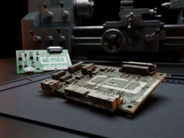
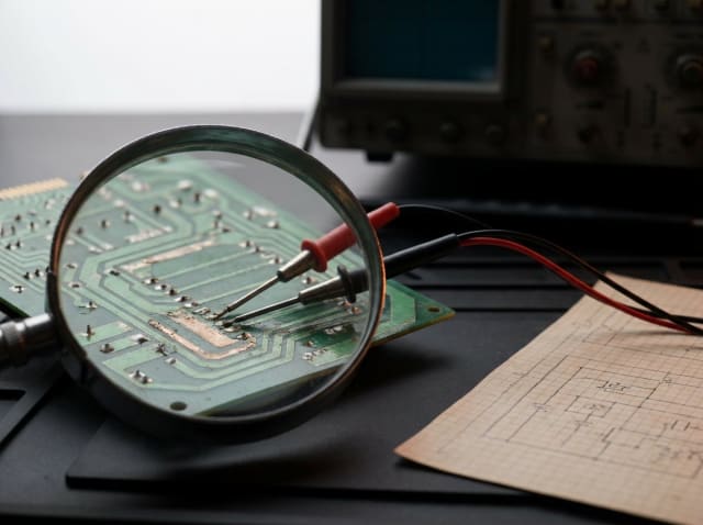
The work starts with reconstructing the schematic: the board is traced under a microscope, components are identified, the circuit is rebuilt. Obsolete parts are then replaced with modern equivalents — which often means delivering the same function with fewer components.
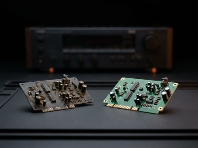
The result is a new PCB revision with full documentation. The device is no longer hostage to an unobtainable part: next time it is needed, you simply order another batch.
How we work
What this area covers
- Board tracing and schematic recovery
- EEPROM / flash dump, reading and analysis
- Modern replacements for obsolete components
- Protocol sniffing — UART, SPI, I²C, CAN
- BOM reconstruction and sourcing
- Signal analysis with logic analyzer and oscilloscope
- Full documentation of the recovered design
- Migrating legacy equipment to a modern controller
What you receive
- Reconstructed schematic, with source file
- Component identification and modern equivalents list
- New PCB design and manufacturing files
- First prototype and functional comparison test
- Difference document — old versus new revision
- A complete document set for future batches
Technologies we work with
From concept to production
- 01
Consultation and Requirements Analysis
We jointly define the project's goals, functional requirements, and budget/timeline constraints. NDA signed if needed.
- 02
Architecture and Schematic Design
System architecture, part selection, schematic drafted. Initial BOM and PCB block diagram agreed upon.
- 03
PCB Layout and Firmware
PCB design (KiCad/Altium), signal integrity, EMC checks. Firmware developed in parallel. Interim reviews.
- 04
Prototype and Testing
First PCB batch assembled and lab-tested. Validation with firmware. Required adjustments.
- 05
Production and Support
DFM optimization for mass production. Documentation, user manual, long-term technical support.
Frequently asked questions
Other engineering areas
Have an idea? Let's talk
Small prototype, medium-scale R&D, or long-term technical support — regardless of your project size, I respond within 48 hours.