
PCB Design and Schematic Capture
PCB design services in Baku — schematic capture, multilayer PCB layout in KiCad and Altium, signal integrity, EMC and DFM review. Gerbers, BOM and assembly documents delivered.
Typical project:4-layer sensor PCB· 2–5 weeks
Project
Tell us briefly about the project: what you want to build, which functions it needs, the rough timeframe. If we have done something similar we will send an example.
Schematic and PCB layout — KiCad and Altium. Signal integrity, EMC, DFM principles.
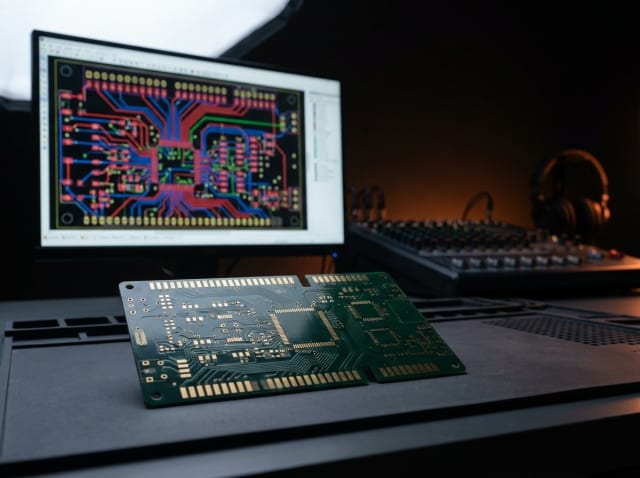
PCB design does not end with drawing the schematic — whether a board works in the real world depends on the layout. Power plane splits, grounding, length matching on high-speed lines and component placement cannot be fixed afterwards; they are either right from the start, or the board misbehaves once it comes back from the fab.
We work in KiCad and Altium. Parts are chosen against real availability while the schematic is drawn — a component that is perfect on paper but unobtainable stops the project. During layout we review signal integrity, EMC readiness and DFM, because a single rule violation can send a whole batch back from the factory.
As often as a design from scratch, we are asked to redraw an existing board: a component has gone end-of-life, the outline has to change, or the old design has a persistent fault. In those cases we start from the existing schematic and build a new revision on top of it.
How we work
What this area covers
- Schematic drafting (KiCad, Altium)
- 2–8 layer PCB layout
- Signal integrity and EMC design
- DFM (Design for Manufacturing) checks
- BOM preparation and part selection
- Gerber, IPC, Pick-and-Place files
What you receive
- Schematic — source file and PDF
- PCB layout file — KiCad or Altium
- Gerber, drill and pick-and-place files
- BOM with sourcing links
- 3D model and mechanical fit check
- Assembly drawing and test notes
- DFM report against the factory's rules
- The project files are yours — free to reuse in later revisions
Technologies we work with
From concept to production
- 01
Consultation and Requirements Analysis
We jointly define the project's goals, functional requirements, and budget/timeline constraints. NDA signed if needed.
- 02
Architecture and Schematic Design
System architecture, part selection, schematic drafted. Initial BOM and PCB block diagram agreed upon.
- 03
PCB Layout and Firmware
PCB design (KiCad/Altium), signal integrity, EMC checks. Firmware developed in parallel. Interim reviews.
- 04
Prototype and Testing
First PCB batch assembled and lab-tested. Validation with firmware. Required adjustments.
- 05
Production and Support
DFM optimization for mass production. Documentation, user manual, long-term technical support.
Frequently asked questions
Other engineering areas
Have an idea? Let's talk
Small prototype, medium-scale R&D, or long-term technical support — regardless of your project size, I respond within 48 hours.