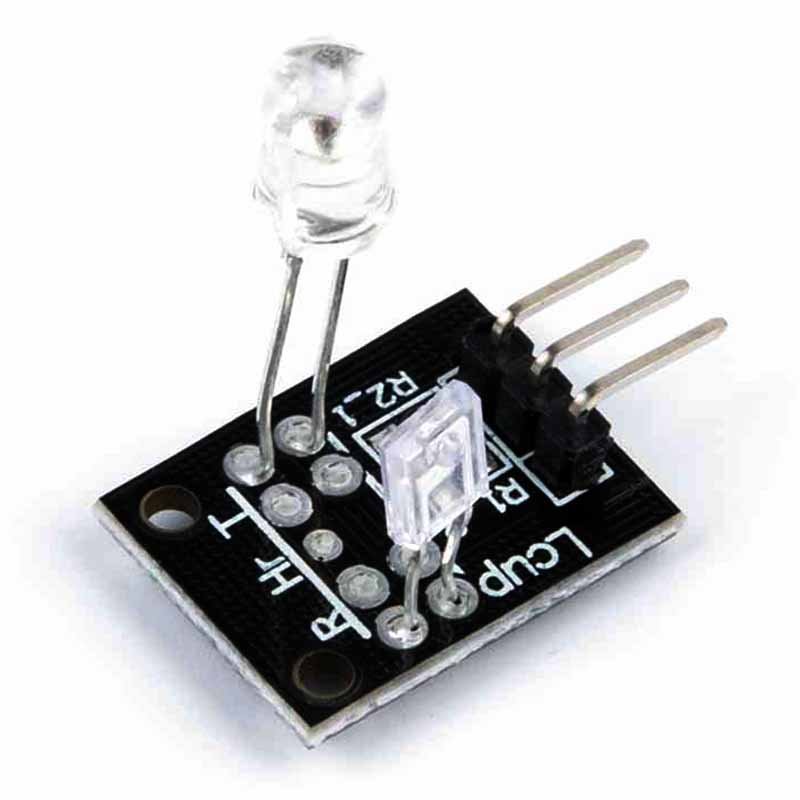
Every Arduino blink sketch, every STM32-based motor controller, every Wi‑Fi module you solder onto a PCB has the same microscopic hero inside: the transistor. For embedded engineers it’s not abstract history – it’s the physical switch that makes our designs possible.
Let’s walk through the key milestones that turned a lab curiosity into trillions of MOSFETs in your pocket.
1947–1954: The birth of the solid‑state switch
On December 16, 1947, at Bell Labs, John Bardeen, Walter Brattain, and William Shockley demonstrated the first point-contact transistor built on germanium. They were trying to replace bulky, fragile vacuum tubes with something smaller, cooler, and more reliable.
The first transistor was:
- a chunk of germanium with two closely spaced metal contacts,
- operating only at low frequencies,
- extremely sensitive to assembly details and not production‑friendly.
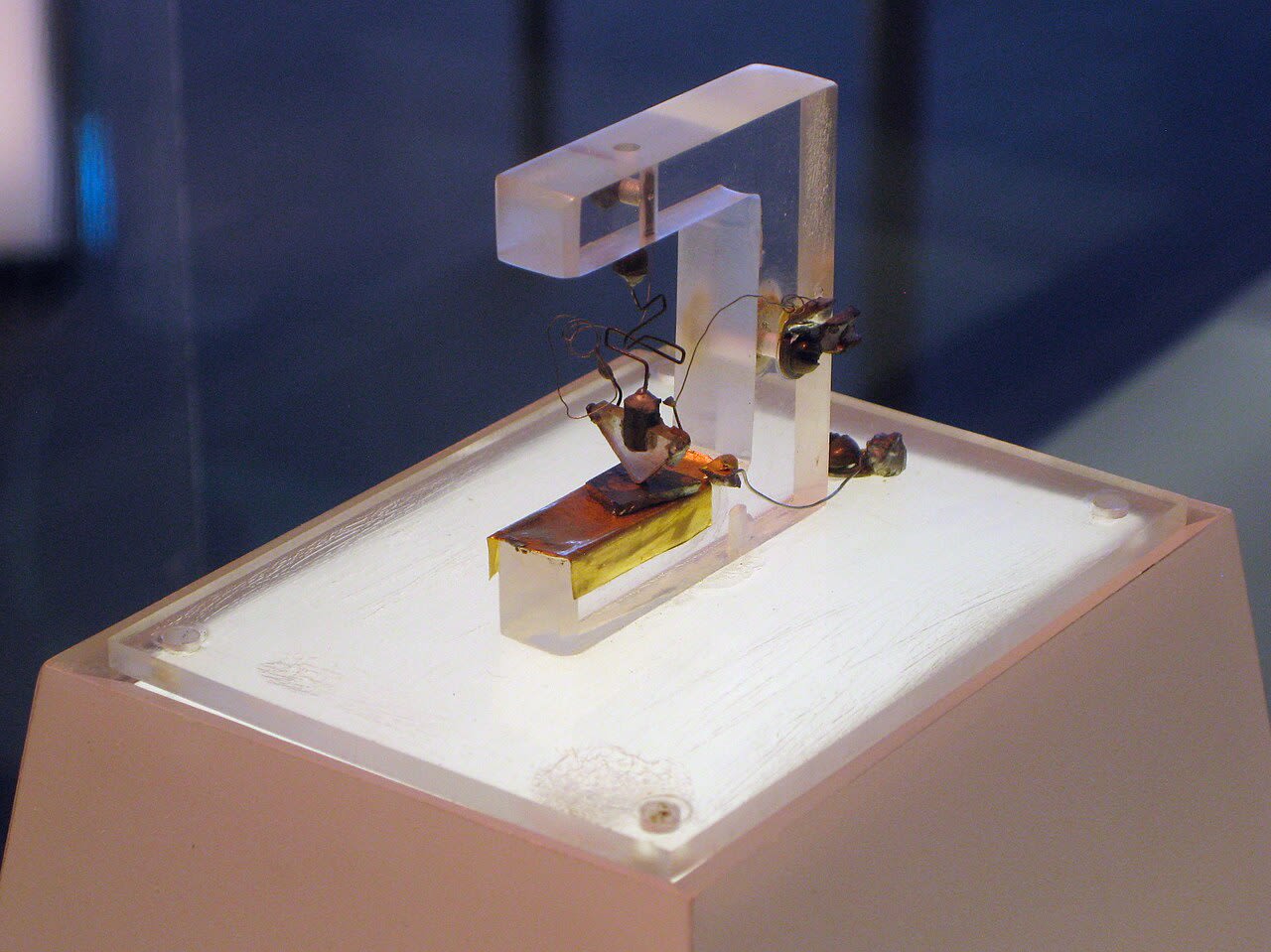
Replica of the first point-contact transistor, invented at Bell Labs in 1947 — Image: Windell Oskay from Sunnyvale, CA, USA / Wikimedia Commons, CC BY 2.0
In 1951–1954, the bipolar junction transistor (BJT) with grown/diffused junctions emerged. In 1954, Texas Instruments shipped the first commercial silicon BJT. Silicon’s better thermal stability and oxide technology made it the real industrial workhorse.
For the first time, amplification, switching and logic could be done without heaters, vacuum, and kilovolt supplies.
1954–1970: Transistor radios and the first ICs
In 1954, the Regency TR‑1 became the first commercial pocket transistor radio. Instead of a handful of glowing tubes, it used a few germanium transistors and ran from a 22.5 V battery. Portability was the selling point – and the public loved it.
But wiring dozens of discrete transistors was still painful. Around 1958–1959, Jack Kilby (TI) and Robert Noyce (Fairchild) independently demonstrated the integrated circuit (IC): multiple transistors and passive components fabricated on a single piece of semiconductor.
In 1960, the first working MOSFET (Metal‑Oxide‑Semiconductor FET) was reported. Compared to BJTs, MOSFETs offered:
- almost zero DC input current,
- much higher integration density,
- an easier path to scaling down.
That was the seed of modern CMOS – the technology behind nearly every microcontroller and SoC we use.
1971–1990: Microprocessors and Moore’s law in action
In 1971, Intel 4004 arrived: a 4‑bit microprocessor with about 2,300 transistors, built on a 10 µm process. It ran at a few hundred kHz and powered calculators – yet it proved you could put a CPU on a single chip.
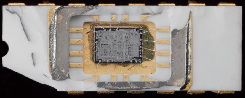
Intel 4004 microprocessor with its ceramic casing partially removed to show the silicon die. — Image: the Science Museum / Wikimedia Commons, CC BY 4.0
Soon came:
- Intel 8080 (1974) – 8‑bit, ~6,000 transistors,
- Intel 8086 (1978) – 16‑bit, ~29,000 transistors,
- Motorola 68000 (1979) – ~68,000 transistors.
Moore’s law, formulated in 1965, observed that the number of transistors on an IC roughly doubled every 18–24 months. By 1989, the Intel 80486 already packed around 1.2 million transistors.
In this era, the transistor:
- moved from discrete packages into invisible on‑die structures,
- shifted the design focus from analog building blocks to digital architecture.
The classic 8‑bit microcontrollers that still dominate hobby embedded – MCS‑51, PIC, AVR – grew directly out of this microprocessor wave.
1990–2010: Nanoscale CMOS and the consumer explosion
By the early 1990s, desktop CPUs entered the multi‑million transistor era. The Intel Pentium (1993) had about 3.1 million transistors on a 0.8 µm process. Over the next decade, process nodes shrank rapidly: 180 nm → 130 nm → 90 nm → 65 nm → 45 nm.
Transistor counts skyrocketed, but cost per transistor kept falling. That made it economically viable to embed:
- full 32‑bit cores in cheap microcontrollers,
- DSP blocks, USB, Ethernet MACs on the same die,
- large flash and SRAM arrays next to logic.
At the same time, power transistors made their own leap:
- MOSFET H‑bridges made PWM motor control easy for hobby robots,
- IGBT modules became standard in industrial drives, solar inverters, and EV powertrains.
Your Arduino UNO’s ATmega328P only needs tens of thousands of transistors, but it sits in a world where billions per chip are routine – and that ecosystem keeps its price under a few dollars.
2010–today: FinFETs, 3D structures and billions on a fingernail
Around 2011, Intel introduced 22 nm FinFET technology into mass production. Unlike planar MOSFETs, a FinFET raises the channel as a thin “fin” and wraps the gate around three sides, improving control over the channel.
Benefits:
- lower leakage current at small geometries,
- higher switching speed,
- better scalability below 30 nm.
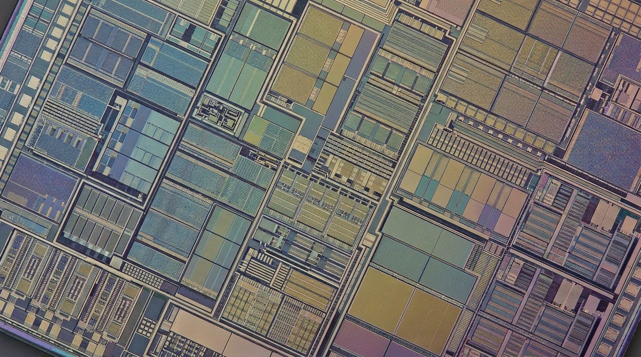
Modern CPU die – billions of nanoscale transistors on a single chip — AI-generated illustration
Today’s flagship chips illustrate just how far we’ve come:
- Apple M1 (2020) – about 16 billion transistors, 5 nm,
- high‑end GPUs – on the order of 50–80 billion transistors.
Compare that to 1971:
- Intel 4004: 2,300 transistors, ~10 µm, hundreds of kHz,
- a modern ESP32: millions of transistors, 240 MHz dual‑core, Wi‑Fi, Bluetooth, flash interface, ADCs, DACs, all on a few mm² of silicon.
For embedded designers, this means we now routinely get:
- MCU + radio + security in a single SoC,
- ultra‑low‑power sleep modes thanks to optimized CMOS,
- high‑voltage, high‑current MOSFETs in compact packages for motor and power control.
What’s next: Beyond classic CMOS
As we push below 5 nm, traditional planar scaling runs into physics limits: leakage, variability, quantum effects. Research is exploring:
- GAAFET / nanosheet transistors for sub‑5 nm nodes,
- 2D materials like graphene and MoS₂ for ultra‑thin channels,
- new device concepts like tunnel FETs, spintronic devices, and memristors.
Whatever comes next, the pattern is clear: more transistors per chip, closer to the sensors and actuators we control. For the embedded world, the transistor’s evolution is what keeps pushing computation, connectivity, and power electronics directly onto the same tiny board you route in KiCad.